Adc analog converter conversion signal converters dac done sample sampling device converted Adc dual block diagram converter digital slope analog integrating indicating pic work mcu works functionality shown below Diagram block embedded world
Block diagram of the proposed ADC architecture | Download Scientific
Analog to digital converter (adc)
Adc block diagram (simplified).
Block diagram of generic adc1: block diagram of adc design Block diagram for adc interfaceAdc bit comparator converter analog microcontrollerslab negative.
[diagram] 8051 adc block diagramAdc dac guid Analog to digital converter (adc) block diagram, workingBasic block diagram of conventional adc[1].

Adc msps sar multiplexer input
Block diagram of the proposed adcBlock diagram of n-bit flash adc architecture Getting started with adc(a) block diagram of the adc. (b) simplified schematic of stages #1 to.
Adc embedded diagram module block lab registers ansel channelsBlock diagram of the proposed adc architecture Adc hardware block diagramBlock diagram for adc interface.

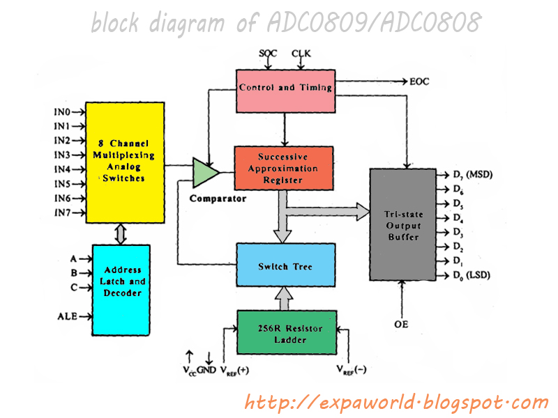
World of embedded: block diagram of adc0809/adc0808
Functional block diagram of a modern 1-msps sar adc with 8-channelAdc dac diagrama digikey analog cna bloques schéma fonctionnel approximation successive Adc block diagram analog cortex shot pm screen ti previous itemBlock diagram of the adc architecture..
Adc successive diagram block approximation sar circuit digital converter analog capacitor sample sa convertor circuits decimal segment display full dischargeDelta-sigma adc basics: walking around the delta-sigma blocks Sar adc block diagram3-bit flash analog to digital converter with example circuit.

Analog to digital conversion (adc)
Functional block diagram of wilkinson adc.Adc block diagram figure Adc block diagram ppt powerpoint presentation bitAdc block diagram counter analog type digital conversion figure.
Adc block simplifiedAdc block diagram using system Adc block diagramAdc – fasoc: fully-autonomous soc synthesis using customizable cell.

Block diagram of the proposed adc architecture.
Adc block convertor analog digital diagramAnalog to digital converter Ti tm4c123 adc blockAdc/dac tutorial.
.